Transistor PPT | PowerPoint presentation | PDF: The transistor is a terminal device and the three terminals are base, emitter, and collector. The input signal of small amplitude is applied at the base to get the magnified output signal at the collector. A BJT is made up of a silicon crystal or germanium crystal in which a thin layer of n-type silicon is sandwiched between the two layers of p-type silicon.
Transistor PPT | PowerPoint presentation | PDF
This type of transistor is known as PNP. Similarly, in an NPN transistor, a layer of p-type material is sandwiched between the two layers of n-type material. The diagrammatic representation of NPN and PNP transistors are as below:
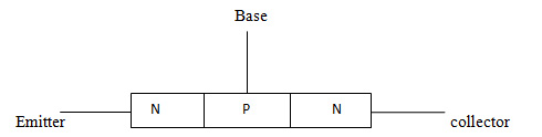
Fig1: NPN Transistor
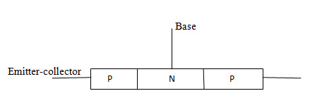
Fig2: PNP Transistor
The transistor is a three layered semiconductor machine and the three layers are an emitter, base, and collector. The emitter is a heavily doped layer, a base is moderately doped and the collector is lightly doped. The doping of the sandwiched layer is less when compared with the outer layers. The conductivity decreases because of the lower doping level as it limits the number of free electrons. The term bipolar reflects the truth that holes and electrons participate in the process of injection into the material which oppositely polarized. In the transistor, the current of a collector is comprised of minority components and majority components.
Transistor Current Components:
There are distinct components which flow across the forward biased emitter junction and the reverse biased collector junction. The emitter consists of the current due to holes and electron current from the base into the emitter. The ratio of hole to electron current crossing the emitter junction is proportional to the ratio of the conductivity of the p-material to that of an n-material. All the holes do not cross the emitter junction and reach the collector junction because few holes combine with the electrons in the n-type base. If the emitter is open circuited so that = 0 then would be zero and under these conditions, the base and collector act as a reverse biased diode and the collector current would equal to the reverse saturation current .
The Operation of the Transistor:
A transistor is said to be properly biased if the loop of base and collector is reverse biased and the loop of base and emitter is forward biased. The width of the depletion layer will be decreased because of the applied biased between the base and emitter which results in a heavy flow of majority carriers from p-type material to the n-type material. Because of the applied reverse biased between the base and collector, the width of the depletion layer increases and this avoids the flow of majority carrier.
When we apply the forward bias and reverse bias then a large number of majority carriers diffuses across the forward biased p-n junction into the material of n-type. The n-type material which is sandwiched has low conductivity as it is very thin and less number of flux carriers will take a path of high resistance to the terminal of a base. Across the reverse biased junction and into the material of p-type which is connected to the terminal of a collector, a large number of majority carriers diffuses. The emitter current is equal to the sum of base current and collector.
Transistor Configurations:
The three distinct types of BJT configurations are explained below:
- Common base configuration
- Common emitter configuration and
- Common collector configuration
- Common base configuration: The common base configuration of an NPN transistor, the input is forward biased and whereas the output is reverse biased. In the configuration of common base, a base is common to the input side of configuration and also to the output side of configuration.
- Common emitter configuration: The input characteristics and output characteristics of the common emitter configuration neatly explain the detailed operation of the common emitter configuration.
- Common collector configuration: The input characteristics and output characteristics plays a major role in knowing the detailed operation of the common collector configuration.
Content of the Seminar and PDF Report for Transistor
- What is a Transistor?
- Evolution of transistor
- Importance of transistor
- Definition & transistor types
- Transistor symbol & operation
- Advantages of transistor
- Latest in transistor technology
- References
Here we are giving you Transistor Seminar and PPT with PDF report. All you need to do is just click on the download link and get it.
Transistor PPT and Seminar Free Download
Transistor PDF Report Free Download
It was all about Transistor Seminar and PPT with pdf report. If you liked it then please share it or if you want to ask anything then please hit comment button.