Download MOSFET Seminar | PPT | PDF Report
Download MOSFET Seminar | PPT | PDF Report: The abbreviation of metal oxide semiconductor field effect transistor is MOSFET. BJT is a bipolar device and in this, the conduction takes place through the electrons and holes. Field effect transistor i.e. FET is a unipolar device and in this, the conduction takes place through the electrons or holes. For the unipolar devices, an electric field is established by the existing charge and it will control the output’s conduction path.
In the controlling of the conduction path of output, it doesn’t need any controlled quantities and controlled quantities. The high input impedance is one of the most important features of the field effect transistor and they are not more sensitive to the changes in the input like the BJT’s.
Also See: Semiconductors PPT and PDF Report
Download MOSFET Seminar | PPT | PDF Report
Types of Field Effect Transistors:
There are two types of field effect transistors and they are explained below:
- JFET i.e. junction field effect transistor
- MOSFET i.e. metal oxide semiconductor field effect transistor
The MOSFETs are again Classified as below:
- Depletion MOSFET and
- Enhancement MOSFET
1. Depletion MOSFET: In depletion MOSFET, the controlling electric field decreases the number of majority carriers available for conduction. In the construction of N-channel depletion MOSFET, N-channel is diffused between the source and the drain to the basic structure of MOSFET. The source and drain terminals are connected together through metal contacts to N-doped region linked by N-channel. The gate is connected to a metal contact surface but remains insulated from the N-channel by a thin is equal to zero volts and is applied to source and drain terminals.
The free electrons from the N-channel are attracted towards positive terminals of drain terminal. If we apply negative gate voltage, the negative charges on the gate repel conduction of electrons from the channel and attract holes from the p-type substrate. This recombination reduces the number of free electrons in N-channel for the conduction reducing the drain current.
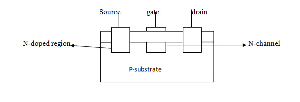
Fig1: n-channel MOSFET – depletion mode
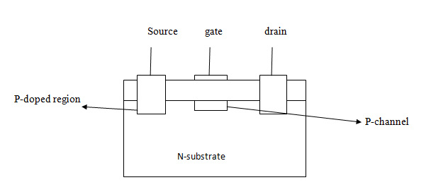
Fig2: p-channel MOSFET – depletion mode
2. Enhancement MOSFET: This type of MOSFET operates in only enhancement mode and has no depletion mode. It differs in construction from the depletion MOSFET is that it has no physical channel.
N-channel enhancement MOSFET: The N-channel enhancement MOSFET has two highly doped n-regions which are diffused into the lightly doped p-type substrate. The source and drain are taken out through metallic contacts to N-doped regions. But the channel between two n-regions is absent. The layer separates the gate metallic platform from source and drain. By giving a voltage and keeping = 0, practically zero current flows.
If we increase a magnitude of in the positive direction then the concentration of electrons near the surface increases. At particular, the value of has a measurable current between drain and source. This value of is called as thread voltage and the channel is established. The conductivity of the channel increases as the increases. For any voltage below the threshold value, there is no channel.
P-channel enhancement MOSFET: The construction of the p-channel enhancement MOSFET is exactly opposite to that of n-channel MOSFET. Here the substrate is of n-type and the regions are of P-type. A positive bias voltage is given between drain and source. Since the channel is not present, the drain current is zero. When a negative voltage is connected between gate and source i.e. at a particular value of called threshold voltage then the channel is established between a source and drain, then the current flows from the drain to source. From the transfer characteristics, it is observed that as the voltage increases in the negative direction, then the current increases as the channel width increases.
Also See: Monorail System PPT, PDF Report
Content of the Seminar and PDF Report for MOSFET
- Introduction
- MOSFET Circuit & symbol
- Working principle
- N & P channel of MOSFET
- MOS Transistor symbol
- Applications
- Advancements and Limitations of the MOSFET
- References
Here we are giving you MOSFET Seminar and PPT with PDF report. All you need to do is just click on the download link and get it.
MOSFET PPT and Seminar Free Download
MOSFET PDF Report Free Download
It was all about MOSFET Seminar and PPT with pdf report. If you liked it then please share it or if you want to ask anything then please hit comment button.

Leave a Reply